The gap waveguide is built up of two parts: a structured metal surface and a flat metal surface being placed in close proximity to one another. The structured surface is characterized by pins forming a barrier preventing the electromagnetic waves from propagating in undesired directions, resulting in signal losses as low as for rectangular waveguides.
可以提供26.5~110GHz的GAP转接波导,产品联系:sales@gamtic.com,021-5197 0121.
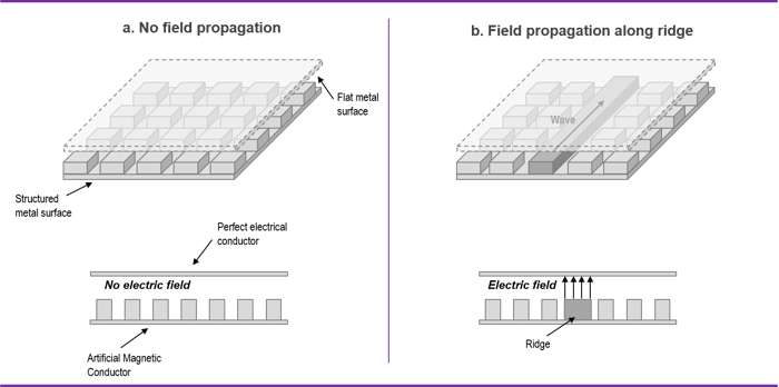
The gap waveguide is built up of two parts: a structured metal surface and a flat metal surface being placed in close proximity to one another (see figure 1). The structured surface is characterized by pins forming a metamaterial surface called an Artificial Magnetic Conductor. The pins create a barrier preventing the electromagnetic waves from propagating in undesired directions. In this way, the pins replace the walls in rectangular waveguides. This is done without requiring a perfectly sealed metallic enclosure. Figure 1a illustrates a scenario with only pins, which shows that no waves can propagate in the structure. However, when ridges are introduced, as shown in figure 1b, waves are allowed to propagate within the pin structure. The waves propagate in the air gap (thereby the name gap waveguide) between the ridges and the top metal surface, resulting in low signal losses. In addition, no metallic contact is required between the two parts, resulting in a much simpler assembly compared to rectangular waveguides that need to be welded or screwed tightly.
 Figure
1. A gap waveguide is built up of a pin structure that prevents the
electromagnetic waves from propagating in undesired directions and
ridges that guide the waves through the structure
Figure
1. A gap waveguide is built up of a pin structure that prevents the
electromagnetic waves from propagating in undesired directions and
ridges that guide the waves through the structure
The open structure of the gap waveguide technology also enables integration of other microwave circuits such as active components. This is done by replacing the flat metal surface by a circuit board making it possible for the gap waveguides to interface directly with the active components.
Comparison with alternative technologies
There are primarily three alternative technologies to gap waveguides: microstrip waveguides, rectangular waveguides and substrate integrated waveguides (SIW) (see Figure 2).
Microstrip waveguides can be produced at a relatively low cost and offer a high design flexibility as they are made using traditional circuit board technology. However, they are lossy at higher frequencies (e.g. at millimeter waves) as the waves travel in a dense medium that absorbs their energy, transforming the signals into heat. When used at frequencies above 20 GHz the losses increases significantly.
Rectangular waveguides have low losses, as the waves travel in a rectangular tube filled with air. However, the technology requires a complex and costly production process using welding or screws. The reason is that the rectangular tubes need to be sealed with a perfect metallic contact to avoid leakage (signal losses).
Substrate integrated waveguides (SIW) are a compromise between microstrip waveguides (in terms of loss) and rectangular waveguides (in terms of cost). As for microstrip waveguides the waves travel in a dense medium (usually a circuit board), but with less energy being absorbed due to the design of the waveguide. However, they still result in losses that limits their use at frequencies above 20 GHz.
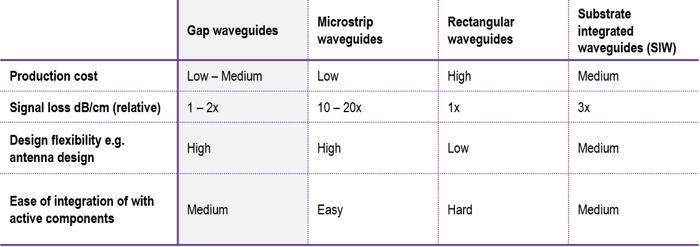 Figure 2. Comparison of gap waveguides and three alternative waveguide technologies
近日,电子科技大学自动化工程学院研究团队在期刊《神经网络》上发表研究性论文。该文首次提出毫米波近场透视成像与可见光的图像融合方法。随着目标检测技术的快速发展,多种传感器在提升检测精度方面发挥着关键作用......
现代信息社会中,移动通信是实现信息高效流动的基本手段。近期,第五代移动通信系统(5G)已实现大规模商用。当前,5G长期演进和第六代移动通信系统(6G)成为学术界和产业界的研究热点。实现高通量无线通信的......
毫米波(名词解释⏬)与太赫兹波(名词解释⏬)探测技术在通信、安全、生物检测、频谱分析等领域有着广泛的应用。它们是将承载着毫米波与太赫兹波的光信息转变为电信号的核心技术。高灵敏度、宽波段、快速响应及面阵......
近日,由中国科学院沈阳自动化研究所团队与以色列魏茨曼科学院(WeizmannInstituteofScience)研究团队,联合提出了针对多输入多输出(Multiple-InputMultiple-O......
在时间某处,也许就是此刻新一代的技术变革正激发全新理念的诞生作为未来科技的推动者我们帮助从事前沿研究的高校、公司、研究机构,开启测量新视野使其产品从概念到商用,速度更快科技的迅猛发展带来了很多新的变化......
今日推荐文章作者为东南大学毫米波国家重点实验室主任、IEEEFellow著名毫米波专家洪伟教授,本文选自《毫米波与太赫兹技术》,发表于《中国科学:信息科学》2016年第46卷第8期——《信息科学与技术......
对于投资者来说,军民融合一直是双创中一个重要的领域,由高校实验室走出的项目往往具有高精尖等特点。但是另一方面,这些项目往往都是军转民,而且项目长期处于高校之中难以发现。为了提高科技成果转化,支撑产业发......
由北京航空航天大学承担的“新能源汽车”重点专项“电动汽车智能辅助驾驶关键技术研究与产品开发”项目“智能辅助驾驶环境感知关键技术研究与产品开发”课题研究取得阶段性成果。课题重点围绕77GHz毫米波雷达关......
分析测试百科网讯2017年2月23日,国家重大科学仪器设备开发专项“毫米波成像探测仪研制及产业化示范”项目(2012YQ140037)初步验收会在同方威视密云基地召开。国家科技部资源配置司副司长吴学梯......
意大利电信近日宣布成立一个毫米波(mmWave)频段实验室,用于研究毫米波在5G网络中的应用。意大利电信是欧洲第一家开设毫米波实验室的电信运营商。这个位于都灵的实验室包括远场紧凑天线测试系统和球面近场......